Meizhou Optimal Processing of Double Conductive Copper Foil
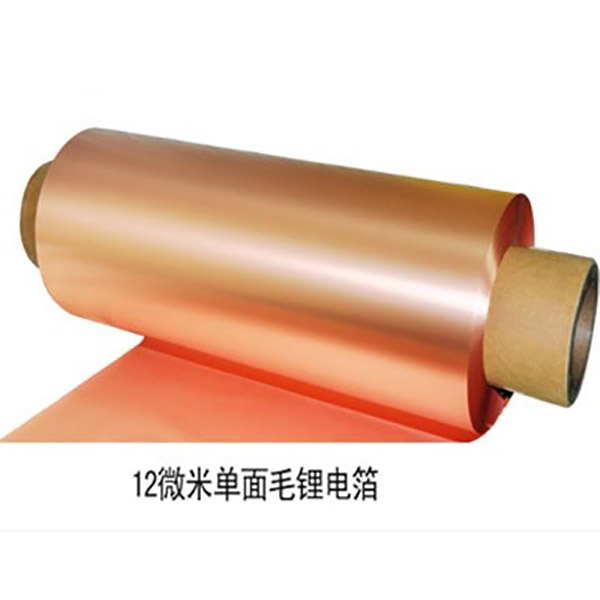
Copper foil can also be divided into: single-sided treatment (single-sided hair), double-sided treatment (double-sided thick), smooth treatment (double-sided hair), double-sided light copper foil (double-sided hair) and very low profile copper foil (VLP copper foil) according to the surface condition. Post copper foil can be divided into electrolytic copper foil and calendered copper foil according to different production methods.
Meizhou Optimal Processing of Double Conductive Copper Foil
During the production of copper foil, tiny foreign matters are adhered on the surface to form spots with different colors from the surface, which are called stains. Judgment method: use macroscopic inspection to judge whether it is a waste product, a secondary product or a finished product according to the number and area of stains and the impact on product quality.
Meizhou Optimal Processing of Double Conductive Copper Foil
Electronic circuit copper foil plays an important role in conducting electricity and heat in printed circuit board (PCB), and is known as the neural network on PCB. At present, copper foil for electronic circuits (PCB copper foil) is divided into two categories, namely conventional copper foil and high-performance copper foil.
Meizhou Optimal Processing of Double Conductive Copper Foil
The surface of the copper foil shall be smooth and clean without obvious wrinkles, oxidation spots, scratches, pitting, pits and stains. The porosity of 305g/m2 and above shall not exceed 8 penetration points within the area of 300ram × 300mm; The total area of pores on an area of 0.5m2 shall not exceed the circular area with a diameter of 0.125mm.
Meizhou Optimal Processing of Double Conductive Copper Foil
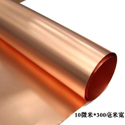
Most copper foils used for domestic printed boards are 35um thick, and 50um copper foils are used as transition products. In high-precision hole metallized double-sided or multilayer board manufacturing, thinner than 35um copper foils, such as 18um, 9um and 5um copper foils, are expected. Some multilayer boards use thicker copper foil, such as 70um.