Zhuhai Optimal Processing of Double Conductive Copper Foil
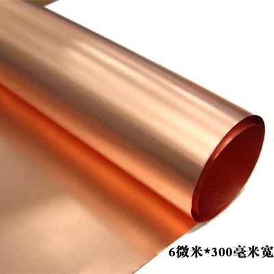
The ultra-thin copper foil, represented by mobile phones and laptops, is promoted to thin foil and ultra-thin foil types for portable electronic products, including micro buried, blind hole L multilayer boards, and BGA, CSP and other organic resin packaging substrates. At the same time, COz laser etching also requires the substrate to be extremely thin, so that the copper foil layer can be directly machined with micro wire holes. In Japan, the United States and other countries, electrolytic copper foils of 9 μ m, 5 μ m and 3/- tm can be industrialized. At present, the difficulty or key point of the production technology of ultra-thin copper foil is whether it can be directly produced without carrier, and the product qualification rate is high, as well as the development of new carriers.
Zhuhai Optimal Processing of Double Conductive Copper Foil
The production process of electrolytic copper foil is simple. There are three main processes: solution raw foil, surface treatment and product slitting. The production process seems simple, but it is a production process that integrates electronics, machinery and electrochemistry, and is particularly strict with the production environment. Therefore, the industry does not have a set of standard and universal production equipment and technology, and each manufacturer shows its own ingenuity, which is also an important bottleneck affecting the improvement of domestic production capacity and quality. In addition, the different requirements of customers have also resulted in the waste of many intermediate products copper foil in manufacturing. The one-time input-output ratio is even less than 80%, and these copper foils have to be manufactured again, wasting resources.
Zhuhai Optimal Processing of Double Conductive Copper Foil
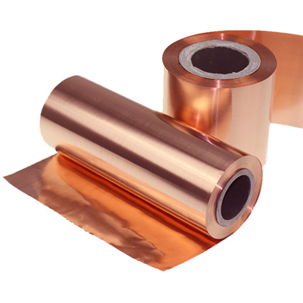
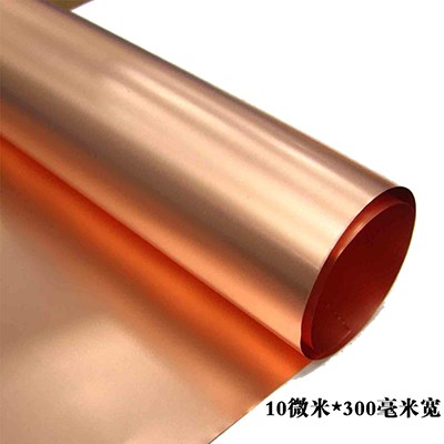
Copper foil can be divided into many kinds according to different classifications. According to the thickness, it can be divided into: thickness (more than 70 μ m) Regular thickness copper foil (more than 18 μ M but less than 70 μ m) Thin copper foil (more than 12 μ M but less than 18 μ m) Ultra thin copper foil (less than 12 μ m) Etc.
Zhuhai Optimal Processing of Double Conductive Copper Foil
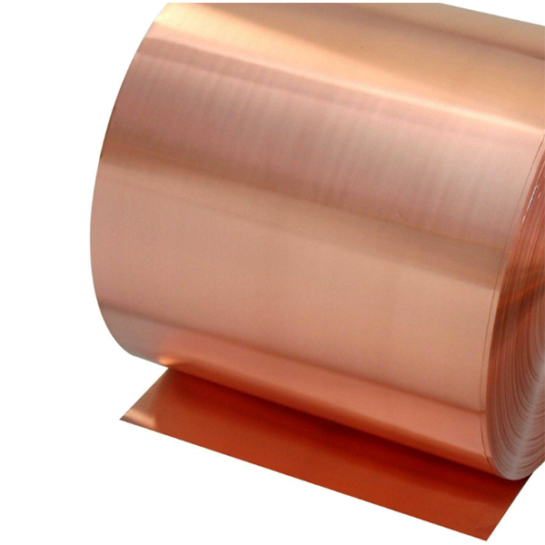
The surface of the copper foil shall be smooth and clean without obvious wrinkles, oxidation spots, scratches, pitting, pits and stains. The porosity of 305g/m2 and above shall not exceed 8 penetration points within the area of 300ram × 300mm; The total area of pores on an area of 0.5m2 shall not exceed the circular area with a diameter of 0.125mm.
Zhuhai Optimal Processing of Double Conductive Copper Foil
With the development of high-density wiring technology for low profile copper foil multilayer boards, the traditional type cannot meet the needs of manufacturing high-precision printed circuit boards. Therefore, a new generation of copper foils, low profile (LP) and ultra-low profile (VLP), have emerged one after another. Compared with ordinary electrolytic copper foil, LP copper foil has fine crystal (2/zm), equiaxed grains, no columnar crystals, lamellar crystals, flat prisms and low surface roughness.