Hefei Optimum Anti static Copper Foil Processing
Most copper foils used for domestic printed boards are 35um thick, and 50um copper foils are used as transition products. In high-precision hole metallized double-sided or multilayer board manufacturing, thinner than 35um copper foils, such as 18um, 9um and 5um copper foils, are expected. Some multilayer boards use thicker copper foil, such as 70um.
Hefei Optimum Anti static Copper Foil Processing
The surface of the copper foil shall be smooth and clean without obvious wrinkles, oxidation spots, scratches, pitting, pits and stains. The porosity of 305g/m2 and above shall not exceed 8 penetration points within the area of 300ram × 300mm; The total area of pores on an area of 0.5m2 shall not exceed the circular area with a diameter of 0.125mm.
Hefei Optimum Anti static Copper Foil Processing
Curing treatment: deposit a layer of dense metal copper in the nodular particle gap of the roughening layer, increase the contact surface between the roughening layer and the wool foil substrate, and reduce the roughness of the roughening layer surface. Microscopically, after rough surface roughening treatment, the foil surface is uneven and undulating greatly, while after curing treatment, the copper foil surface is relatively flat. After curing treatment, although the roughness is reduced, the bonding strength between the treatment layer and the insulating substrate material is improved due to the increased contact area between the roughened layer and the wool foil, which fundamentally eliminates the delamination between the treatment layer and the wool foil.
Hefei Optimum Anti static Copper Foil Processing
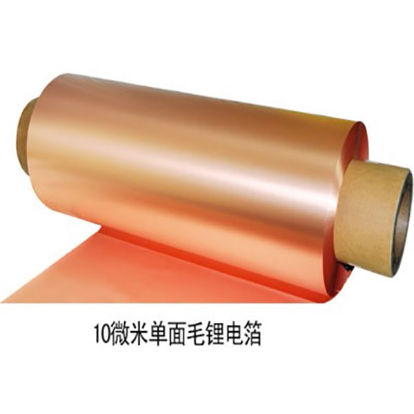
Copper foil is a key conductive material in lithium ion batteries and printed circuit boards. It is a kind of negative electrolytic material, a thin, continuous metal foil deposited on the substrate of circuit board.